
Improving At-Speed Test Coverage without Compromising Test Time and Reducing Test Cost in Multi-Partition SCAN Design
Introduction
The ongoing progress in semiconductor technology has resulted in the development of highly integrated System on Chip (SoC) designs that amalgamate digital, analog, and memory elements. This heightened complexity presents challenges in guaranteeing reliable manufacturing, particularly in identifying production defects. In the realm of Very Large Scale Integration (VLSI), testing plays a vital role in maintaining design integrity prior to the products being delivered to end users. Techniques such as Design-for-Testability (DFT) have become crucial for enhancing the testability of intricate circuits by incorporating additional logic during the design phase, thereby facilitating effective fault detection after silicon fabrication.
A commonly employed DFT technique is SCAN-based testing, which utilizes scan chains to improve the controllability and observability of internal circuit components, including flip-flops and latches. SCAN cells are arranged in a series configuration, enabling the shifting of test patterns in and out, thereby improving the identification of both structural and functional defects through the use of Automatic Test Pattern Generation (ATPG) tools.
At-speed testing serves as an essential enhancement to SCAN-based testing, concentrating on the identification of timing-related defects that arise during standard operational conditions. This testing approach replicates real operating speeds to uncover transition delay faults that might remain undetected in static scenarios. Nevertheless, at-speed testing presents certain challenges, particularly in terms of maintaining test coverage within the limitations of Automated Test Equipment (ATE), which is constrained by its memory and processing power.
To tackle these challenges, sophisticated DFT methodologies are utilized to enhance controllability and observability, thereby enabling efficient testing of each partition without overburdening ATE memory. The fundamental concepts encompass:
Design-for-Testability (DFT): Methods integrated into a chip’s architecture to enable effective fault identification.
At-Speed Transition Coverage: Assesses a circuit’s capability to switch between states at its real operating speed.
A System-on-Chip (SoC): integrates various functional elements into a single chip, necessitating advanced testing procedures.
Automated Test Equipment (ATE): Equipment specifically designed for testing chips after manufacturing.
Integrated Clock Gating (ICG): Regulates power consumption in digital circuits by controlling the activation and deactivation of clock signals.
Test Compression (EDT): Minimizes the volume of test data through on-chip compression and decompression techniques.
Launch-on-Shift (LOS): Identifies delay faults by initiating test data during the scan shift phase.
SCAN Design: Integrates sequential components into scan chains to facilitate regulated access during testing.
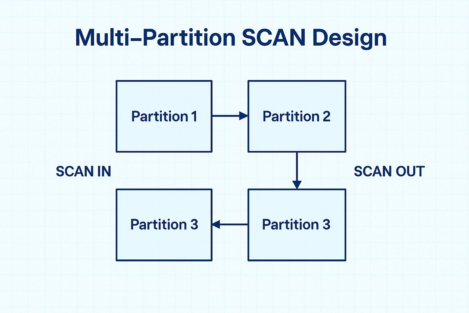
Partitioning Method: Segments the System on Chip into manageable sections to facilitate efficient testing.
Wrapper cells and EXTEST chains: facilitate the isolation and verification of interfaces between different partitions.
Test Points (TP) Registers: Enhance visibility and control to improve fault detection capabilities.
This paper focuses on meeting at-speed transition coverage requirements within ATE memory limitations, exploring DFT techniques and proposing a novel architecture for improved at-speed coverage and reduced test time/cost.
Motivation
As SoC technology advances, integrating digital, analog, and memory components increases testing complexity. Detecting manufacturing defects, especially those arising in high-speed operations, requires robust DFT strategies and high at-speed transition fault coverage for reliable SoC functionality.
Numerous research efforts have investigated methods to improve System on Chip (SoC) fault coverage, emphasizing the reduction of memory usage and the optimization of testing procedures. For instance, advancements in Motorola’s microprocessor design resulted in more effective test pattern generation and enhanced fault detection capabilities. The optimization of test patterns for gigahertz microprocessors has increased coverage while adhering to Automated Test Equipment (ATE) limitations. Additionally, the enhancement of scan flip-flops and modifications to Register Transfer Level (RTL) have contributed to greater efficiency in at-speed testing.
A major challenge is ATE memory limitations, as both uncompressed and compressed pattern sets can require excessive memory. Overcoming these constraints while maintaining high fault coverage is a key goal.
Recent advancements have presented novel architectures, including creative state assignments and enhanced inter-core IO testability, aimed at minimizing pattern counts and testing duration while maintaining precision. This research seeks to build upon these principles to enhance at-speed transition fault coverage for intricate System on Chips (SoCs) under stringent memory and testing time limitations.
Methodology
This section is organized into three sub-sections: architectural details, analysis of the problem, and DFT methodologies aimed at addressing deficiencies in at-speed transition coverage concerning the memory requirements of external testers.
A. Architecture Details
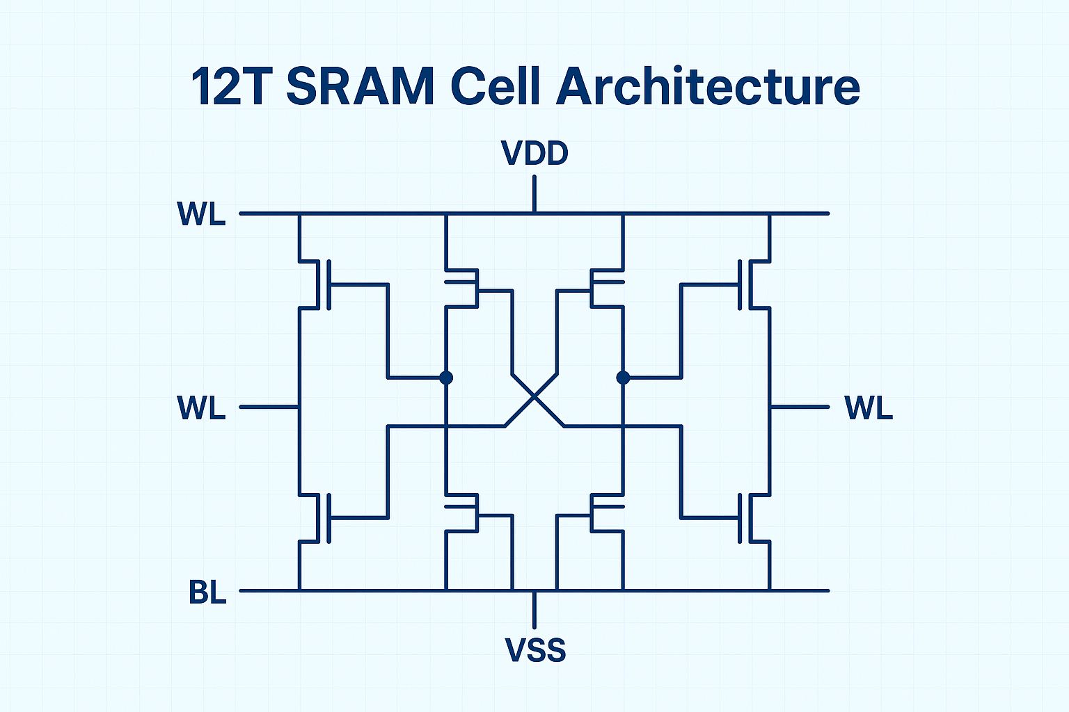
This project involves a System on Chip (SoC) design utilizing TSMC’s 16nm technology node, incorporating an ARM CPU, a secure cryptographic processor, and various peripherals such as GPIO, QuadSPI, and UART. The memory architecture comprises 30 instances of SRAM and 2 instances of ROM. The Design for Test (DFT) strategies encompass JTAG/iJTAG interfaces, 200 test point registers, a partitioned SCAN design, test compression logic (EDT), and a low-power feature within the compression logic. The SoC operates with 30 clock domains and approximately 400,000 scan flip-flops.
B. Problem Analysis
The initial coverage for at-speed transition testing was approximately 80% utilizing production test patterns; however, this necessitated around 250MB of ATE memory, significantly surpassing the 20MB limit. The objective was to achieve 90% coverage while adhering to the 20MB memory restriction, thereby minimizing both test duration and expenses.
C. DFT Techniques to Improve At-Speed Coverage
a). Analyzing Coverage Loss Surrounding Memory:
The loss of coverage was attributed to uncontrolled control signals within memory blocks, frequently produced by secure circuitry and not directly managed by the testing unit. Additionally, signal duplication during the physical design phase further exacerbated the coverage loss.
b). Proposed Solutions:
The paper details solutions for resolving these issues, including architectural changes and disabling certain low-power features during test mode to reduce pattern count and test time without exceeding power budgets.
Conclusion
This study illustrates that by examining key aspects like memory-adjacent logic and ICG enable logic, along with the application of architectural advancements and strategic optimizations, it is possible to reach the at-speed coverage target of 90% while adhering to strict ATE memory limitations. These approaches improve testing efficiency, lower expenses, and guarantee the dependability of intricate SoC designs.
Authors
Jay K Gohil – ASIC DFT Engineer, Inaved Semicon Pvt. Ltd.
Ramesh B Devani – ASIC DFT Dept., Inaved Semicon Pvt. Ltd.
Jayesh Popat – ASIC DFT Engineer, Inaved Semicon Pvt. Ltd.
Contact: info@inaved.com
Share: